KLA-Tencor Introduces Key Systems for 5D™ Patterning Control Solution
Accelerating The Ramp Of Advanced Patterning Techniques For Sub-20nm Design Nodes
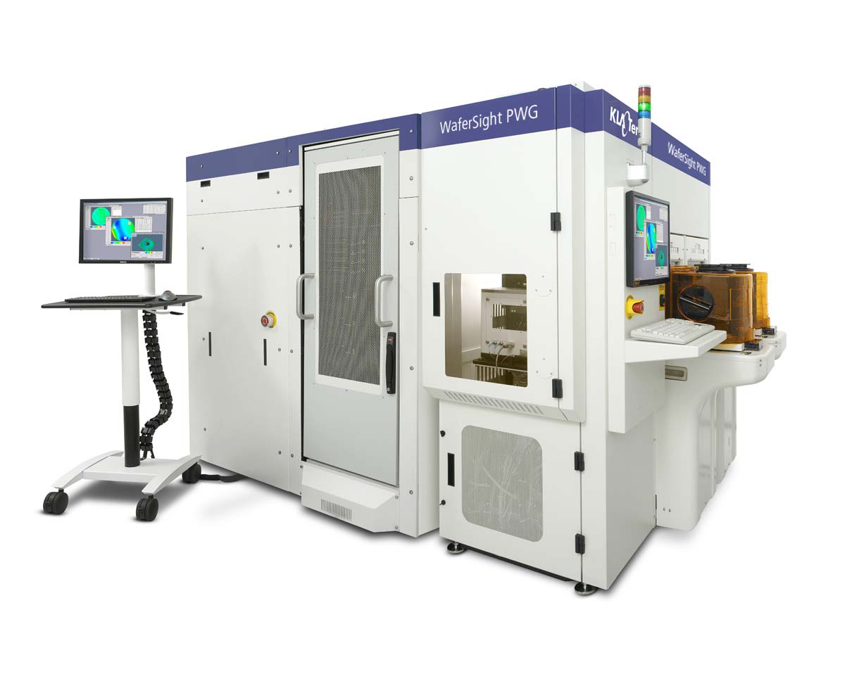
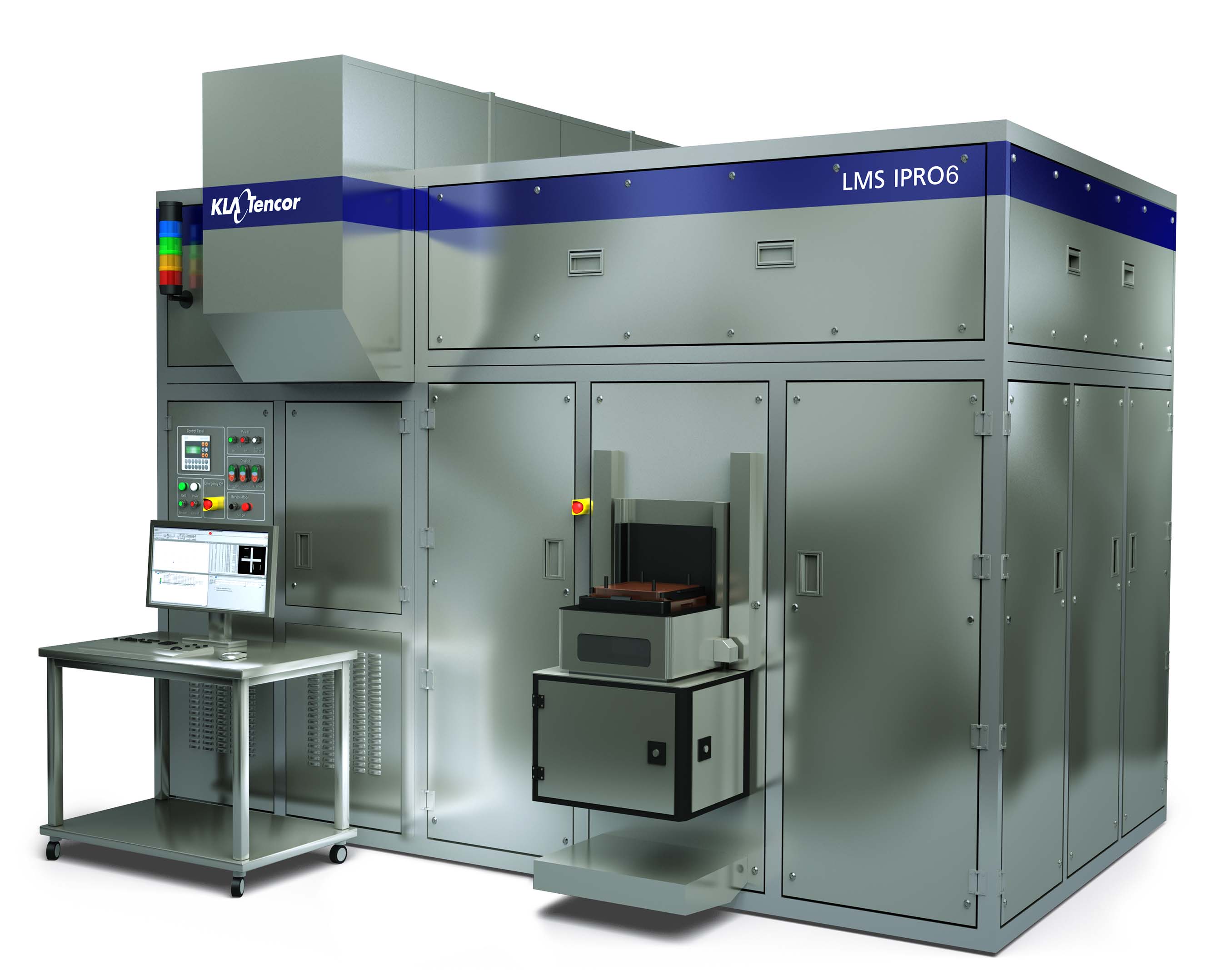
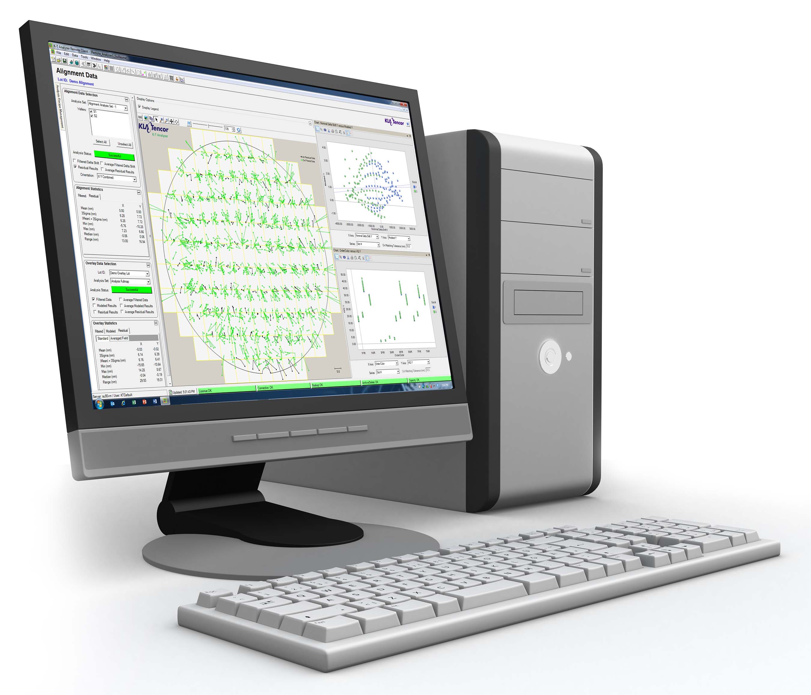
MILPITAS, Calif., Aug. 26, 2014 /PRNewswire/ -- Today, KLA-Tencor Corporation (NASDAQ: KLAC) introduced the WaferSight™ PWG patterned wafer geometry measurement system, the LMS IPRO6 reticle pattern placement metrology system and the K-T Analyzer® 9.0 advanced data analysis system. These three new products support KLA-Tencor's unique 5D™ patterning control solution, which addresses five elements of patterning process control—the three geometrical dimensions of device structures, time-to-results and overall equipment efficiency. The 5D patterning control solution is being developed to drive optimal patterning results through the characterization, optimization and monitoring of processes inside and outside the lithography module. By combining these measurements with intelligent feedback and feed forward process control loops, this solution can help chipmakers obtain faster, more cost-effective ramps of multi-patterning, spacer pitch splitting and other advanced patterning technologies using existing process equipment.
To view the multimedia assets associated with this release, please click: http://www.multivu.com/players/English/7065552-kla-tencor-wafersight-5d-patterning-control-solution/
Logo - https://photos.prnewswire.com/prnh/20140123/SF50413LOGO
"Process control serves a fundamental role in helping our customers navigate the near-zero process windows, shrinking overlay error budgets and other complexities associated with innovative patterning techniques," said Ahmad Khan, group vice president of KLA-Tencor's Parametric Solutions Group. "Within the lithography module, our Archer™ 500 overlay and SpectraShape™ 9000 critical dimension advanced metrology systems identify and monitor patterning errors. Extending beyond the lithography cell, our new WaferSight PWG and LMS IPRO6 systems isolate additional process- or reticle-related sources of patterning errors. These fab-wide, comprehensive measurements, supported by K-T Analyzer 9.0's flexible data analysis, expand the process window and enable improved production patterning control for our customers' leading-edge devices."
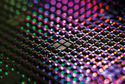
Installed at multiple IC manufacturers for development and production of advanced devices, the WaferSight PWG measures patterned wafer geometry after a wide range of processes, helping chipmakers identify and monitor variations that affect patterning. By incorporating industry-unique vertical wafer hold to minimize gravitational distortion and a sampling density of 3.5 million data points per wafer, the WaferSight PWG produces highly accurate wafer shape data that can be fed forward to the lithography module for wafer shape-optimized scanner corrections that improve pattern overlay. The WaferSight PWG also uniquely measures the wafer's front and back surfaces concurrently, generating wafer thickness metrics that are used to help reduce wafer-induced scanner focus errors. The WaferSight PWG is based on the WaferSight platform, which has strong adoption by worldwide wafer manufacturers for bare wafer geometry quality assurance.
The LMS IPRO6 is being used by leading-edge mask shops for comprehensive characterization of reticle pattern placement error—a direct contributor to wafer-level pattern overlay error. Proprietary model-based metrology allows the LMS IPRO6 to accurately measure reticle registration for on-device pattern features, as well as standard registration marks, offering significantly higher sampling for improved decisions on mask quality. With faster measurement time than its predecessor, the LMS IPRO6 supports the productivity required to qualify the increased number of reticles associated with innovative multi-patterning techniques. The LMS IPRO6 enables generation of pattern-dependent registration error data that improves feedback to the e-beam mask writer and can be fed forward to the fab's lithography module for feature-optimized scanner corrections that improve wafer-level patterning.
Installed at foundry and memory manufacturers, K-T Analyzer 9.0 is the latest version of the industry standard platform that enables advanced, run-time data analysis for a wide range of metrology system types, including overlay, reticle registration, wafer geometry, films, critical dimension and device profile metrology systems. K-T Analyzer 9.0 includes in-line methods for calculating scanner corrections per exposure on an on-product, lot-by-lot basis that maintains high accuracy without requiring full wafer measurement data—a production-capable control technique that can reduce pattern overlay error. In addition, K-T Analyzer 9.0 includes new scanner fleet management, scanner data analysis and scanner alignment optimization capabilities, offering chipmakers a flexible solution for improving scanner utilization and for monitoring and optimizing lithography processes.
WaferSight PWG, LMS IPRO6 and K-T Analyzer 9.0 are part of KLA-Tencor's comprehensive 5D patterning control solution, which also includes overlay, films, critical dimension and device profile metrology systems and the PROLITH™ lithography and patterning simulator. To maintain the high performance and productivity demanded by leading-edge IC manufacturing, the WaferSight PWG, LMS IPRO6 and K-T Analyzer 9.0 systems are backed by KLA-Tencor's global, comprehensive service network. More information can be found on the 5D patterning control solution web page.
About KLA-Tencor:
KLA-Tencor Corporation, a leading provider of process control and yield management solutions, partners with customers around the world to develop state-of-the-art inspection and metrology technologies. These technologies serve the semiconductor, LED and other related nanoelectronics industries. With a portfolio of industry-standard products and a team of world-class engineers and scientists, the company has created superior solutions for its customers for more than 35 years. Headquartered in Milpitas, Calif., KLA-Tencor has dedicated customer operations and service centers around the world. Additional information may be found at http://www.kla-tencor.com (KLAC-P).
Forward Looking Statements:
Statements in this press release other than historical facts, such as statements regarding the expected performance of the WaferSight PWG, LMS IPRO6 and K-T Analyzer systems and the 5D patterning control solution; the extendibility of the WaferSight PWG, LMS IPRO6 and K-T Analyzer systems and the 5D patterning control solution to future technology nodes; trends in the semiconductor industry and the anticipated challenges associated with them; expected uses of the WaferSight PWG, LMS IPRO6 and K-T Analyzer systems and the 5D patterning control solution by KLA-Tencor's customers; and the anticipated cost, operational and other benefits realizable by users of WaferSight PWG, LMS IPRO6 and K-T Analyzer systems and the 5D patterning control solution, are forward-looking statements, and are subject to the Safe Harbor provisions created by the Private Securities Litigation Reform Act of 1995. These forward-looking statements are based on current information and expectations, and involve a number of risks and uncertainties. Actual results may differ materially from those projected in such statements due to various factors, including delays in the adoption of new technologies (whether due to cost or performance issues or otherwise), the introduction of competing products by other companies or unanticipated technological challenges or limitations that affect the implementation, performance or use of KLA-Tencor's products.


To view the multimedia assets associated with this release, please click: http://www.multivu.com/players/English/7065552-kla-tencor-wafersight-5d-patterning-control-solution/
SOURCE KLA-Tencor Corporation
Released August 26, 2014